The integrated circuits, chips, microchips, IC (Integrated Circuit) or CI (Integrated Circuit), or whatever you want to call them, they are a type of electronic circuits that have made possible the advancement of technology to current levels. Without this invention, computing and telecommunications would probably not be what they are, and electronic and electrical devices would be very different.
Despite their tiny size, and that they are everywhere, these integrated circuits hide great surprises to discover. Here you can learn much more about these Electronic components...
What are integrated circuits?

The integrated circuits are pads of a semiconductor encapsulated and containing a recorded electronic circuit. Depending on the logic family to which they belong, these circuits will be made up of different miniaturized electronic components. For example, they can be diodes, transistors, resistors, capacitors, etc.
Thanks to them it has been possible to develop modern electronics and start a new era given the great integration they allow. In fact, some of today's most advanced chips can integrate up to billions of transistors in a die that is just a few millimeters square.
History of chips
At first, electronics began to use rough vacuum valves similar to conventional light bulbs. These valves were large, very inefficient, they got quite hot, and they broke easily, so it was necessary to replace the blown ones so that the computers and other equipment that had them kept working.
En 1947 would come the invention of the transistor, a piece that would replace the old valves and that would also revolutionize electronics. Thanks to him it was possible to have a solid state device, much more resistant, efficient, and faster than valves. However, some thought they could integrate several of these elements into a single silicon chip. This is how the first integrated circuits in history were created.
Over time, solid state electronics evolved and reduced the size of components, as well as lowering costs. In the late 50s, a Texas Instruments inventor named Jack kilby, it occurred to him to create a semiconductor chip and some wiring that interweaved the different parts. This became the first chip in history, and he would go on to win the Nobel Prize for it.
Almost in parallel, Robert NoyceAt the time, an employee of Fairchild Semiconductor (later one of the founders of Intel), he also developed a similar device, but with great advantages over Kilby's. Noyce had created the idea that would give way to today's integrated circuits. This technology was called planar, and it had advantages over Kilby's mesa technology.
Since then, it has not stopped the evolution and improvement of these components. Costs have plummeted, as have fuel economy and size, while performance and performance have dramatically improved. No other sector has evolved so much, and no other sector has had such a great impact on humanity ...
How are they made?
The procedure of manufacture of integrated circuits it is extremely complex. However, as seen in the video, it can be summarized in a few simpler steps so that people can understand how they are done.
Here i will try summarize the design steps the best possible, without going too deep, since it would give for thousands of articles:
- Be part of a need, an application for which you need to create an electronic circuit.
- A design team is in charge of outlining the characteristics and specifications that the chip should have.
- Then, the design will begin using logic gates and other memory elements, etc., until a logic design is achieved that develops the function for which this chip is designed.
- After this, it will go through a series of steps between which tests and simulations are carried out to determine that it works correctly at a logic level, and even test chips are manufactured to see if they do it physically.
- Once the design stage has been completed, a series of masks for manufacturing are created from the layout of the designed circuit. A pattern is engraved on them so that it can be engraved on the silicon.
- This pattern is used by the foundry or factory, to create the integrated circuits in a semiconductor wafer. These wafers usually contain up to 200 or 300 chips in some cases.
This is as far as the design stage, from the manufacturing side, we have:
- The silicon mineral is obtained from sand or quartz.
- Once it is refined to be ultra-pure, or EGS (Electronic-Grade Silicon), with a level of purity higher than the silicon used in other industries.
- This EGS arrives in the form of pieces at the foundry, where it is melted in a crucible and through a seed crystal it is made to grow using the Czochralski method. So that it is easy to understand, it is similar to how the typical cotton candy is made at fairs, you introduce the stick (seed crystal) and the cotton (molten silicon) sticks and increases in volume.
- At the end of that step, the result is an ingot, a large piece of monocrystalline silicon crystal in the shape of a cylinder. This bar is cut into very thin wafers.
- These wafers go through a series of processes to polish the surface so that they remain unpolluted for the start of production.
- Afterwards, these wafers will go through several repetitive processes to create the chips on them. These processes are of a physical-chemical type, such as photolithography, etching or etching, epitaxial growth, oxidation, ion implantation, etc.
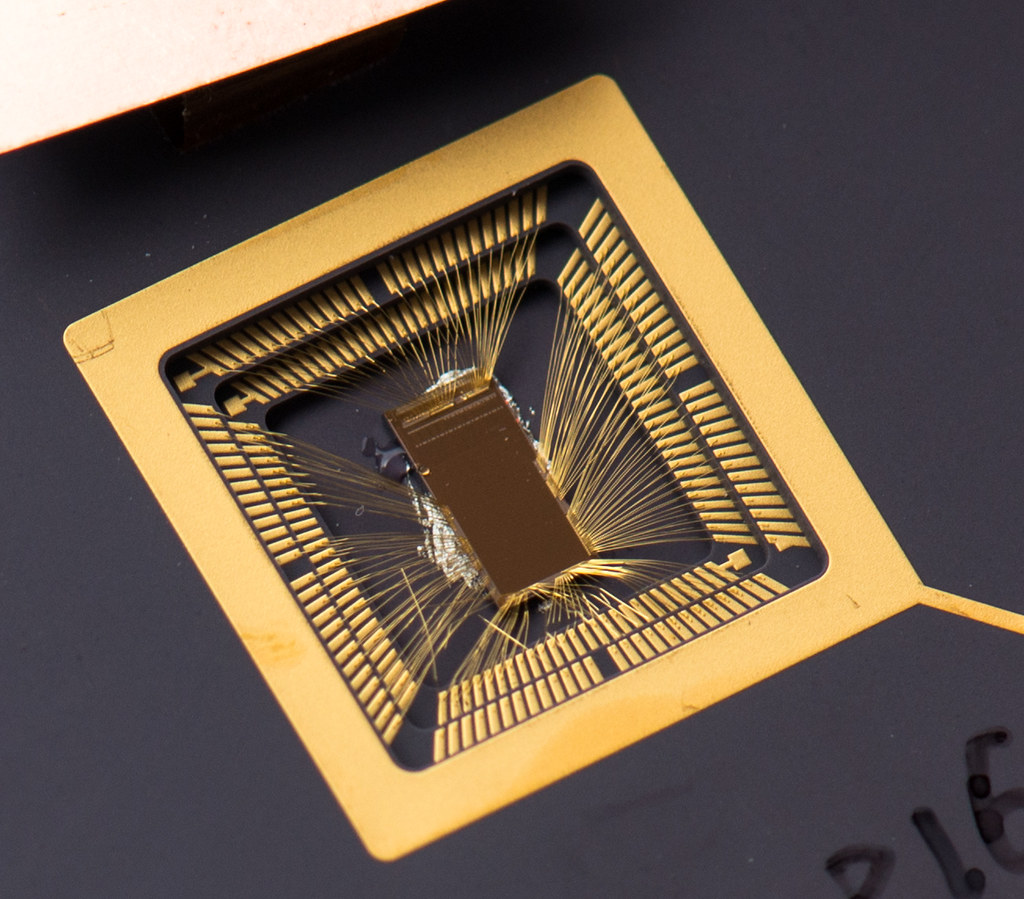
- The final idea is to create electronic components, generally transistors, on the wafer substrate, and then add layers to interconnect said components to form logic gates in the lowest layer, then in the following layers these gates are connected to form elementary units (adders, registers, ...), in the following layers functional units (memory, ALU, FPU, ...), and finally all are interconnected to create the complete circuit, for example, a CPU. On an advanced chip there can be up to 20 layers.
- After all these processes, which can take several months to complete, hundreds of equal circuits will be obtained for each wafer. The next thing is to test and cut them, that is, divide them into individual silicon chips.
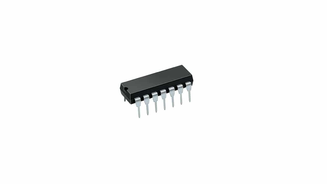
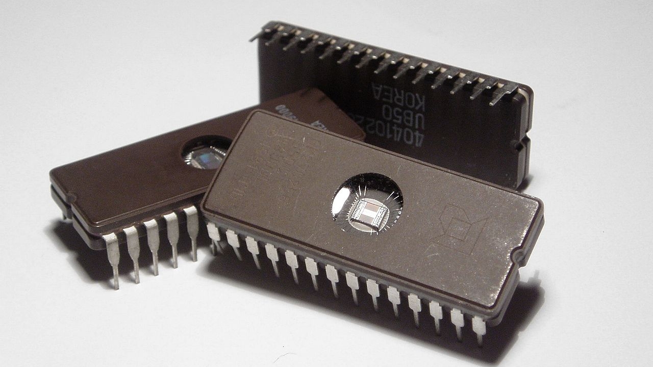
- Now that they are loose dies, we proceed to encapsulate (DIP, SOIC, PGA, QFP, ...) where the chip is protected and the pads are connected, which are conductive tracks on the surface, with the pins of the integrated circuit.
Evidently not all integrated circuits are the same. Here I have talked about functional units and more complex things like a CPU, but there are also very simple circuits like a 555 timer or an IC with 4 logic gates that are extremely simple. They will only have a few dozen components and will be linked with one or a few layers of metallic interconnections ...
Types of ICs
There is not only one type, but several types of integrated circuits. The most prominent ones you can find are:
- Digital integrated circuits: they are quite popular, and used in many modern devices, from computers, to mobile devices, Smart TVs, etc. They are characterized by working based on the digital system, that is, with 0 and 1, with 0 being a low voltage signal and 1 being a high signal. This is how they encode information and operate. Examples can be PLCs, FPGAs, memories, CPU, GPU, MCU, etc.
- Analog: instead of being based on binary signals, in this case they are continuous signals variables in voltage. Thanks to this, they can achieve tasks such as filtering, signal expansion, demodulation, modulation, etc. Of course, many systems work with both analog and digital circuits, making use of AD / DA converters. They can be divided into two large groups, linear integrated circuits and radio frequency (RF). Examples could be a chip for audio filtering, sound amplifiers, emission or reception systems for electromagnetic waves, sensors, etc.
- Mixed signal ICs: as the name suggests, they are a mixture of both. Some examples could be the analog-digital or digital-analog converters themselves, certain chips for clocks, timers, encoders / decoders, etc.
Differences with printed circuits
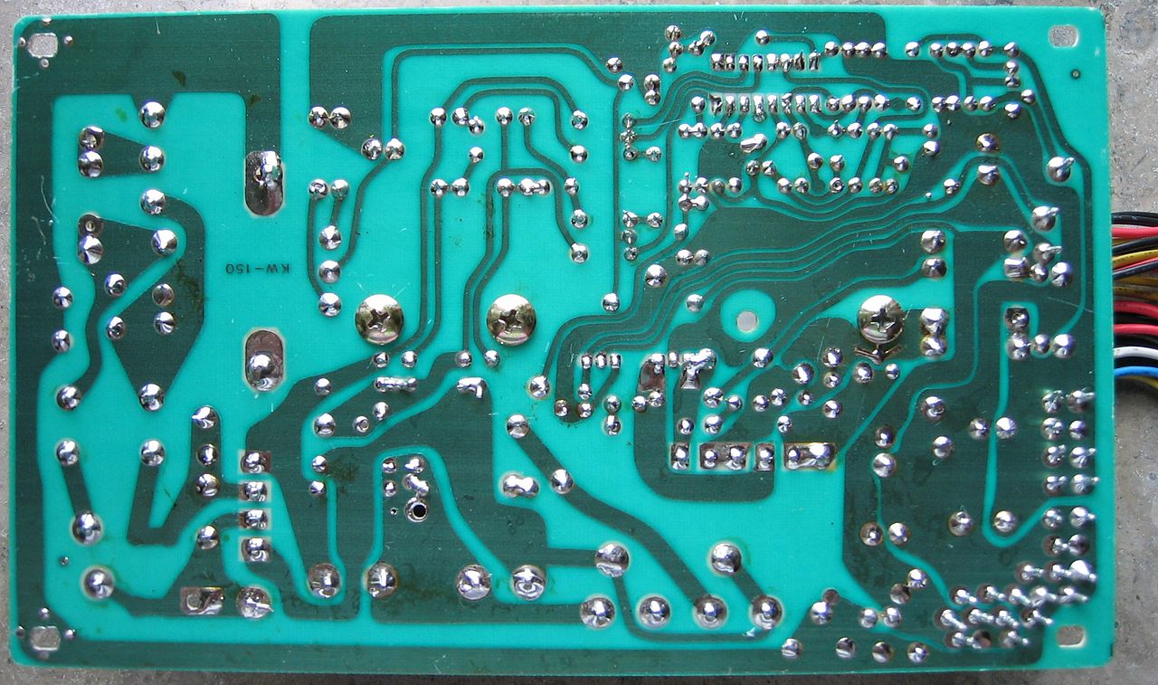
Integrated circuits should not be confused with printed circuits. They are both different things. While the former refer to microchips, as you have seen, printed circuits, or PCBThey are another type of electronic circuits that are printed on larger plates.
All the differences most notable are:
- Printed circuits: they are made up of a plate that has a pattern of conductive lines, such as copper tracks to link the different inserted components (capacitors, transistors, resistors, microchips, ...), soldered by tin soldering, in addition to a dielectric material ( substrate) that separates the layers of connecting interconnections. They also typically have through holes, or vias, for non-surface mount (SMD) components. On the other hand, they usually have a legend, a series of marks, letters and numbers to identify the components and facilitate maintenance. To protect copper, which oxidizes easily, they usually have a surface treatment. And, unlike integrated circuits, they can be repaired, replacing damaged components or restoring interconnects.
- Integrated circuitsThey are very small in size, solid state, and have low cost of mass production. Unlike a PCB, these cannot be repaired as their components and connections are so extremely tiny that it is impossible.
Neither integrated circuits are substitutes for printed circuits nor vice versa. Both have their uses and in most cases they go together in practical applications ...
Most popular integrated circuits
Finally, there are a multitude of very popular integrated circuits employees for electronics projects, such as those of logic gates. They are cheap, and can be easily found in stores like Amazon or specialized electronics. For example, here are some of the most popular:
- 75 popular ICs kit from Interstellar Electronics
- No products found..
- 10 ICs of the popular NE555 timer.
- No products found..