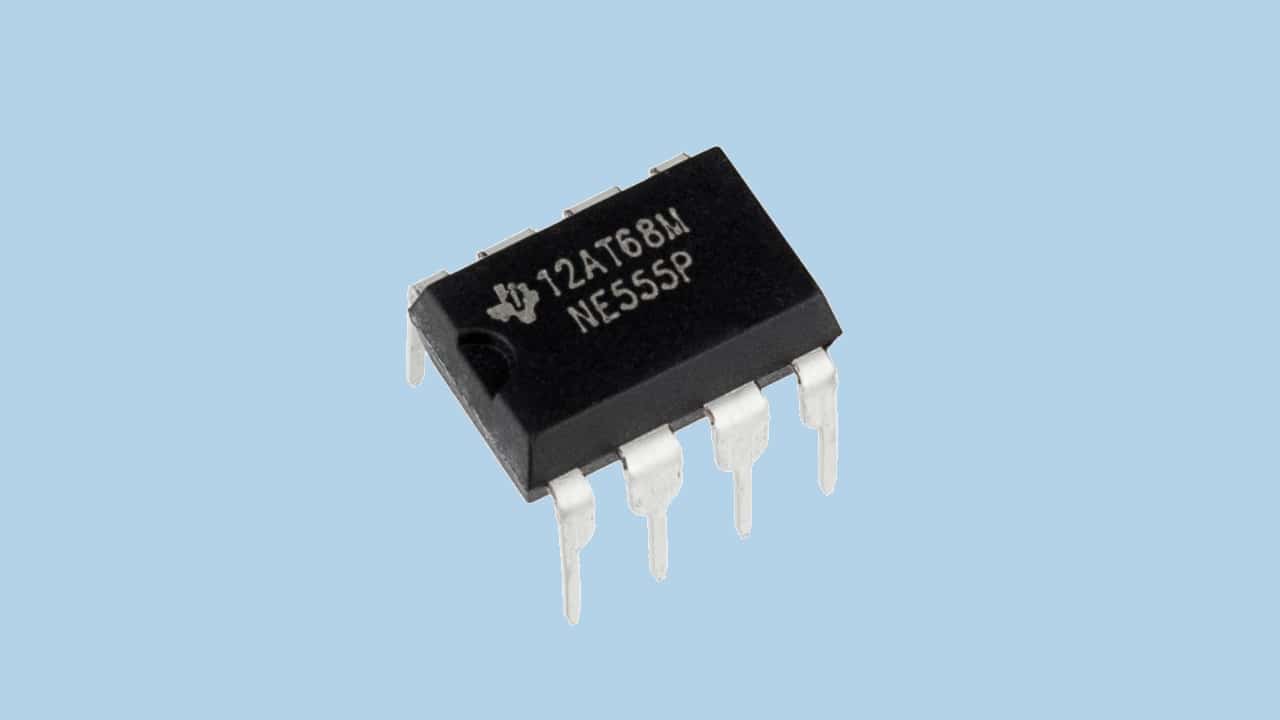
The 555 integrated circuit is one of the most famous chips you will find among the Electronic components. It can come in various forms, such as NE555, NE555C, LMC555, TLC555, uA555, MC1455, LM555, etc. The reason that it is one of the most popular is its versatility, and the number of applications for which it can be used, as you can see here.
In this guide you will learn everything you need about this chip, as well as how to use it in your future projects, recommendations to buy it cheap, etc.
What is the NE555?
The NE555, or simply 555, is an IC used for generate pulses, oscillations or as a timer. Therefore, it can be used as an oscillator, to generate delays, etc. You can generally find it in various packages, although the most common is the 8-pin DIP (there are 14-pin variants), although it can also be in a circular metal package and even in SMD for surface mount.
It is also possible to find versions of the NE555 with low consumption, and even double versions. In these double versions, 2 identical circuits are included inside, with twice as many pins and are usually known as 556.
On a technical level, this circuit must be continuously powered with a Vcc voltage, and the output can have a fairly high current intensity to be an integrated circuit. In fact, this chip could even directly drive relays and other high-drain circuits without the need for additional components. But, it needs a minimum number of external components to be able to function (be controlled).
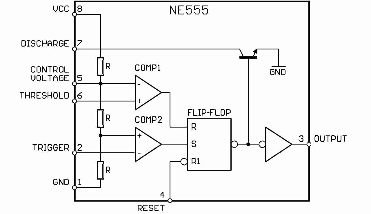
Many will wonder what is what is inside this integrated circuit. Inside the NE555, as can be seen in the previous image, there is a block diagram with two Operational amplifiers mounted as comparators, an RS type bistable circuit making use of its negated output, an inverting output buffer to support that output current, and a transistor used to discharge the external capacitor for timing.
On the other hand, there are also 3 internal resistors that are responsible for setting reference levels of the input of the inverter of the first operational, and in the non-inverting of the second, at 2/3 and 1/3 of the voltage Vcc respectively. Refering to threshold voltage of terminal 6, when it exceeds 2/3 of the supply voltage or Vcc, then the output will go to a high logic level (1) and is applied to the R input of the bistable, so the negated output goes to 1, saturating the transistor and starting the discharge of the external capacitor. Simultaneously, the output of the 555 would go low (0).
En the other op amp, if the voltage applied to the inverting input falls below 1/3 of the Vcc, the amplifier output will go to high level (1), thus feeding the bistable input S, passing its output to low level (0), turning the transistor off and causing the NE555 output to go logic high (1).
Lastly, there is also a terminal reset on pin 4, connected to the R1 input of the bistable flip flop. When this pin is activated logic low (0), it can return the output of the NE555 to low (0) any time a reset is needed.
NE555 Specifications
All the technical specifications of the NE555, although it may vary depending on the versions and the manufacturer, the most common is that you find:
- Vcc or input voltage: 4.5 to 15V (there are versions up to 2V). The 5V ones are compatible with the TTL logic family.
- Input current (Vcc +5v): 3 to 6mA
- Input current (Vcc 5v): 10 to 15mA
- Maximum output current: 500 mA
- Maximum power dissipated: 600 mA
- Minimum power consumption: 30mW@5V and 225mW@15V
- Operating temperature range: 0ºC up to 70ºC. The frequency stability is 0,005% per ºC.
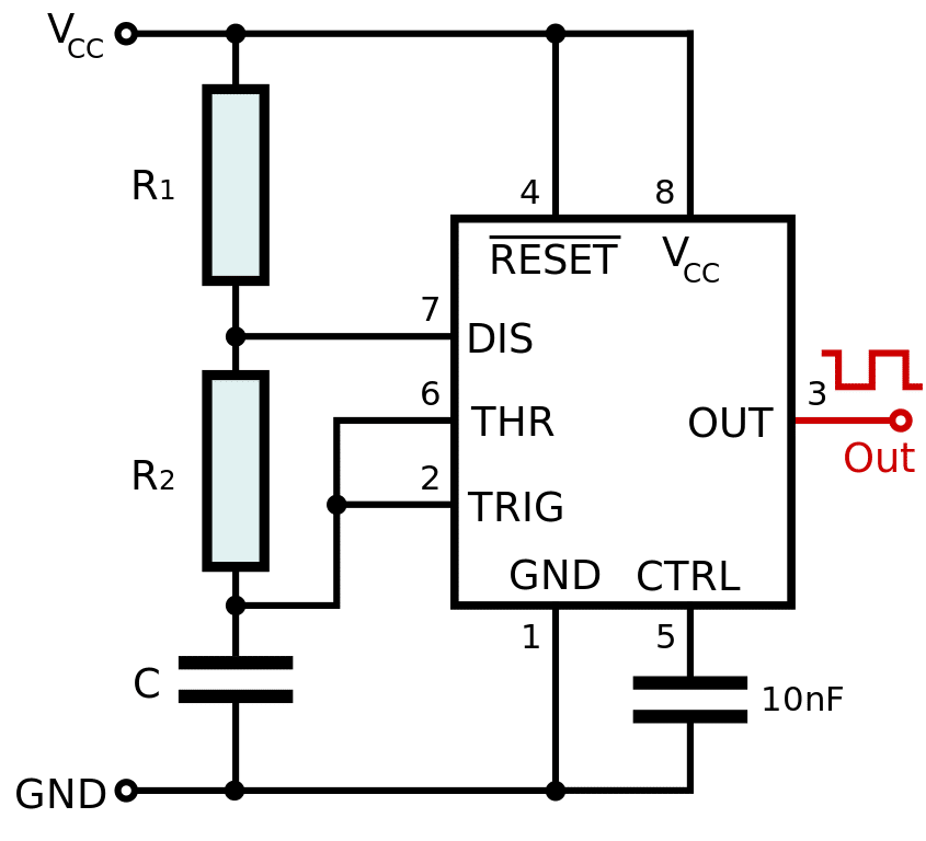
NE555 Pinout
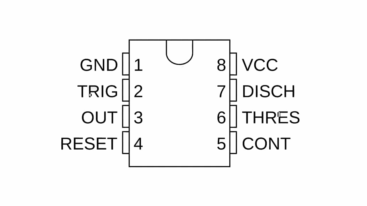
The NE555, in its most common package, has 8 pins. the pinout is:
- GND(1): is the negative pole for the power supply, which generally goes to ground.
- Shot or trigger (2): This pin sets the start of the delay time if it is configured as a monostable. When this pin has less than 1/3 of the supply voltage, the trigger will occur.
- Exit or out (3): is where the result of the timer is obtained, whether in stable mode, monostable, etc.
- Reboot or reset (4): If it goes below 0.7 volts, it will pull the output pin low. If this pin is not used, it should be connected to power to prevent the timer from resetting.
- Voltage control or control (5): When the NE555 is in voltage controller mode, the voltage on this pin will vary from Vcc to almost 0V. In this way it is possible to modify the times, or it can also be configured to generate ramp pulses.
- Threshold or threshold (6): is an input pin for an internal comparator used to pull the output low.
- Download or discharge (7): Used to effectively discharge the external capacitor used for timing.
- Vdc (8): is the supply voltage, the terminal where the chip is fed with voltages ranging from 4.5v to 16v.
Always remember read the manufacturer's datasheet, as there could be differences between the various 555 products. Also, make sure you are using the chip correctly, noting that the notch on the front is facing up to match this pinout.
History of 555
The 555 or NE555 circuit was designed by Hans R. Camenzind in 1971. I was then working for Signetics (currently owned by NXP Semiconductors). Hans already had experience in this type of projects, previously designing amplifiers by pulse width modulation (PWM) for audio equipment, he was also interested in PLLs, etc.
Camenzind would propose to Signetics to develop a world circuit based on PLLs and would ask company management to develop it himself, using company resources in exchange for cutting his salary in half. The company's marketing manager accepted the proposal, despite the fact that other company colleagues claimed that the functionality of the future 555 could be replaced with other existing chips.
The project would take the 5xx numbering assigned to analog ICs. And finally the number 555 would be selected. The first design would be revised in 1971 and, although there were no errors, it had 9 pins. Camenzind had the idea to use a direct resistor instead of a constant current source and reduced the need for pins to the current 8.
The functional design with 8 pins would spend a second design review and the prototype was finally introduced in October 1971. One of the Signetics engineers present at the first review would go on to found another company and make his own 9-pin version. Signetics meanwhile began manufacturing and marketing the NE555 as soon as they could. In 1972 it was manufactured by 12 companies and became one of the best-selling circuits.
NE555 Applications
Between NE555 applications there are those of being a timer or precision timer. Although it was originally presented as a precision delay circuit, it soon found innumerable applications such as serving as an astable oscillator, ramp generator, sequential timer, etc. This is how it became one of the most used chips even today.
555 configurations
All the NE555 configurations they are made with a series of capacitors and resistors connected to their pins. That way you can alter the timing or modes of operation of this IC. Here are some of the most common settings:
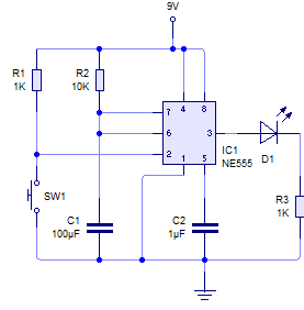
- Monostable configuration: in this case, the output of the NE555 will initially be 0 (low level), and the transistor will be saturated preventing the capacitor C1 from charging. If the button is pressed, a low voltage is applied to the trigger terminal and causes the flip-flop to change state and the output to go to 1 (high level). In that case, the internal transistor stops conducting and the capacitor C1 is charged through the external resistor R1. When the capacitor voltage exceeds 2/3 of the supply voltage (Vcc), the bistable changes its state and the output returns to 0.
- astable: in this other configuration, when it is connected to the power supply, the capacitor is discharged, and the NE555 output goes high (1) until the capacitor reaches 2/3 of the Vcc with its load. At that instant, the RS flip-flop changes level and the 555 output becomes 0 or low. At that instant, the capacitor C1 (or C in the image) begins to discharge through the resistor R2 and when it reaches 1/3 of the supply voltage, it starts charging again and so on while the supply is maintained.
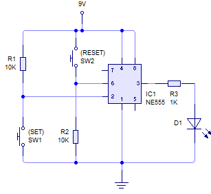
- Configuration for reset: in case you want to reset the circuit, you can connect the reset terminal directly to the positive pole or keep the level high by means of a resistor. When the button shown in the following diagram is actuated, the NE555 will have the output at 0 when desired. It's like restarting the timer or putting it in a sleep state.
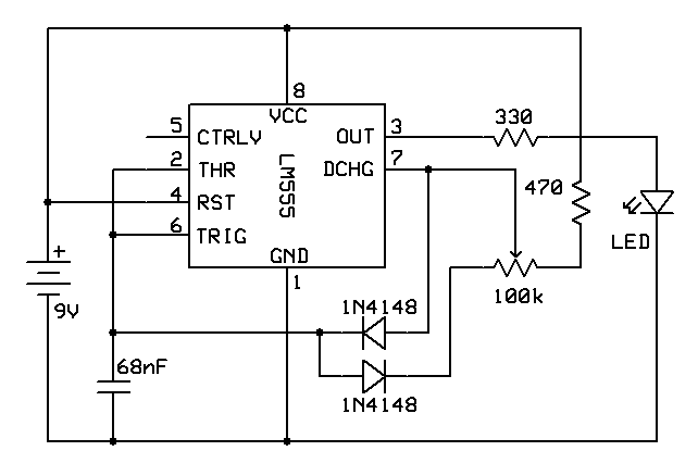
- Pulse Width Modulation (PWM): a variable level signal can be applied to the control input of the NE555, causing the output pulse to increase in width as the level of this voltage increases. The pulse can also be made to arrive with more or less delay as the voltage applied to the control input increases or decreases.
Where to buy the cheap NE555
You can find it in many specialized electronics stores, although it is also easy to find it on Amazon at good prices. Some examples of recommended products are:
- Case with 50 pulse generators NE555P
- NE555 module to be able to use it more easily with Arduino.
- Pack of 10 NE555N units with their corresponding sockets.