![]()
In our electronic components section We have already talked enough about different types of commercial transistors. Now it's time to delve deeper into a widely used transistor, it is the family of BJT transistors, that is, bipolar transistors, so present in many electronic devices that we use on a daily basis.
So you can learn more about these transistors and the differences with unipolar ones...
What is a semiconductor?
-

- SONY DSC

-

- SONY DSC
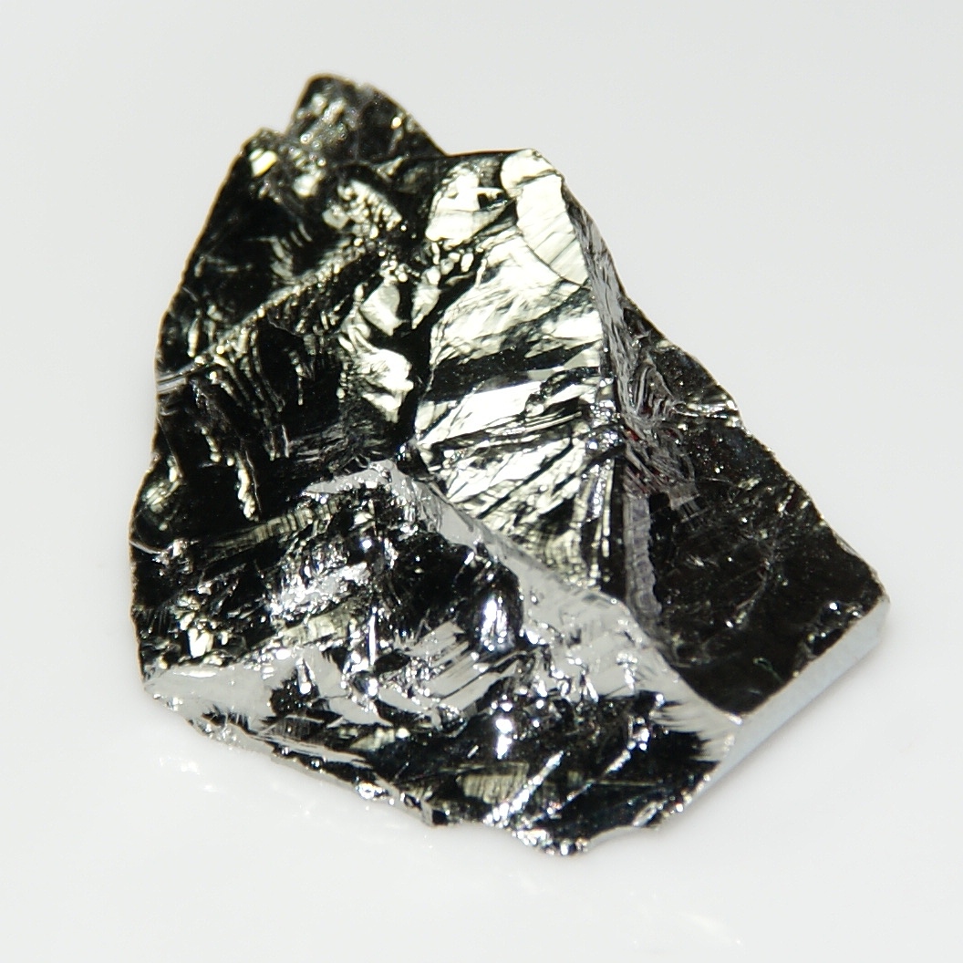
The semiconductors They are materials that have an electrical conductivity between that of conductors and that of insulators. Unlike metals (good conductors) and non-metals (insulators or dielectrics), semiconductors occupy a unique position that allows them to be manipulated to control the flow of electrical current.
Su crystal structure, typically composed of elements such as silicon or germanium, is essential to understanding its behavior. The atoms of these materials form a crystalline structure in which electrons are shared between atoms in energy bands. The valence band contains electrons that are tightly bound to atoms, while the conduction band contains electrons that can move freely.
The semiconductor materials They are essential in the manufacture of advanced electronic devices. Silicon, being one of the most used semiconductors, is ubiquitous in industry and forms the basis of chips and microprocessors. In addition to silicon, germanium is another common semiconductor material that has been used in older technologies. Semiconductor compounds such as gallium arsenide (GaAs) and phosphorene have also gained importance, especially in high-frequency and optoelectronic applications. These materials enable the creation of devices such as light-emitting diodes (LEDs), high-frequency transistors and advanced sensors, demonstrating the versatility and vitality of semiconductors at the forefront of technological innovation.
Cargo carriers and electronic driving
La ability of semiconductors to conduct electricity lies in its ability to generate charge carriers. Charge carriers can be negatively charged electrons or positively charged "holes," which result from electrons that have been shifted from the valence band to the conduction band.
When a voltage is applied to a semiconductor, the electrons can move from the valence band to the conduction band, creating electric current. This phenomenon is known as electronic conduction and is essential for the operation of electronic devices.
Dopants (impurities)
To improve and control the electrical properties of semiconductors, Deliberate impurities are introduced into the glass through a process called doping. The dopant atoms can be of the donor type (adding extra electrons) or of the acceptor type (creating holes), that is, the first would be the so-called N-type semiconductors and the second the P-type semiconductors.
Dopants introduce additional energy levels into the forbidden band, allowing greater control over electronic driving. Some common examples of dopants are phosphorus (donor) and boron (acceptor) for silicon. In this way, zones or junctions can be created to create devices such as a diode, which is basically a single PN junction, or semiconductors, which are usually three zones as we will see later.
Types of Semiconductors: Intrinsic and Extrinsic
On the other hand, to understand the BJT, it is also important to know what types of semiconductors They exist, such as:
- intrinsic: When no impurities are added to a semiconductor, it is classified as intrinsic. In this case, electrical conduction is due solely to the thermal generation of charge carriers (electron-hole pairs).
- extrinsic: They are the result of intentional doping with impurities. N-type (negative) semiconductors are obtained by adding donor dopants, while p-type (positive) semiconductors are formed with acceptor dopants. These processes allow the electrical properties of semiconductors to be adjusted according to the specific needs of the applications.
Introduction to PN junctions

La PN junction It is an essential concept in semiconductor electronics that lays the foundation for the creation of devices such as diodes and transistors. A PN junction is formed when two regions of a semiconductor material come together. These regions are the P-type region (where the concentration of positive charge carriers or holes is predominant) and the N-type region (where the concentration of negative charge carriers or electrons is predominant). The transition between these two regions creates a unique interface with special electrical properties.
La formation of the PN junction It usually occurs through a process called doping, where deliberate impurities are introduced into the semiconductor material. In the P-type region, acceptor dopants (such as boron) are used, while in the N-type region, donor dopants (such as phosphorus) are used, as I mentioned previously. This process creates a concentration gradient of charge carriers across the junction, thus establishing the potential barrier.
As to comportamiento of this PN junction, has unique properties when polarized in different directions:
- En forward polarization, a voltage is applied in the direction that favors current flow through the junction. In this case, the charge carriers move across the potential barrier, allowing electrical conduction.
- On the contrary, in reverse polarization, the applied voltage works against the potential barrier, hindering the flow of current. In this state, the PN junction acts like a diode, allowing conduction in one direction and blocking it in the opposite direction.
The PN junction is the basis of many electronic devices. Diodes, for example, take advantage of the property of the PN junction to allow current flow in one direction and block it in the other. Transistors, fundamental for digital logic and signal amplification, are also built using various PN junctions, as in the case of BJTs that can have NPN or PNP junctions...
What is a BJT transistor?

El bipolar junction transistor (BJT or Bipolar Junction Transistor) It is a solid-state electronic device composed of two very close PN junctions, allowing current increase, voltage decrease, and control of current flow through its terminals. Conduction in this type of transistor involves charge carriers of both polarities (positive holes and negative electrons). BJTs are widely used in analog electronics and some digital electronics applications, such as TTL or BiCMOS technology.
La History of bipolar transistors dates back to 1947, when John Bardeen and Walter Houser Brattain invented the point-contact bipolar transistor at the Bell Telephone Company. Later, William Shockley developed the bipolar junction transistor in 1948. Although they were essential for decades, their use has declined in favor of CMOS technology in digital integrated circuits.
The structure of a BJT consists of three regions:
- The emitter (highly doped and functional as a charge emitter)
- The base (narrows and separates the emitter from the collector)
- The collector (larger extension).
Epitaxial deposition is the common manufacturing technique. In normal operation, the base-emitter junction is forward biased, while the base-collector junction is reverse biased. The operating principle involves the Polarization direct polarization of the base-emitter junction and reverse polarization of the base-collector junction. Electrons are injected from the emitter to the collector, allowing signal amplification. The BJT is characterized by its low input impedance and can be modeled as a voltage-controlled current source or a current-controlled current source.
Bipolar transistor operation
As for operation, we have that in a bipolar junction transistor (BJT) in NPN configuration, The base-emitter junction is forward polarized and the base-collector junction is reverse polarized.. Thermal agitation allows the charge carriers from the emitter to cross the emitter-base potential barrier and reach the collector, driven by the electric field between the base and the collector. In typical operation, the base-emitter junction is forward biased, allowing electrons to be injected into the base region and travel toward the collector. The base region must be thin to minimize carrier recombination before reaching the base-collector junction. The collector-emitter current can be controlled by the base-emitter current (current control) or by the base-emitter voltage (voltage control). In a PNP transistor it is the other way around...
Differences with the unipolar transistor
Transistors can be classified into two main categories: bipolar and unipolar. The key differences What we find between the two are:
- BJT or bipolar: Just like unipolar transistors, bipolar transistors also have positive and negative charge carriers, that is, with P and N doped regions in their structure. As for polarization, they can be polarized directly or reversely, depending on what is needed, and can be NPN or PNP type. As for the operating modes, they can operate in active mode, cut mode and saturation mode. They are current controlled, and have a current gain represented by the letter β (beta). The power loss in this case is higher than that of unipolar transistors and its speed is generally slower than unipolar transistors. Therefore, they are often used in analog signal amplifiers and low-frequency switching, among others. BJTs are more susceptible to noise.
- FET or unipolar: Unipolar or field effect transistors also use charge carriers, but here we have electrons or holes, depending on the type. The main polarization here is the reverse, and the operating modes are mainly in saturation. In this case we have voltage controlled transistors. The current gain is represented in this case by transconductance, the power loss is less than in bipolar ones, and they are faster. For this reason, they are often used for high-frequency switching and digital circuits. Unipolar ones are less susceptible to noise.
BJT type (NPN and PNP)


As I have commented in several parts of the article, there are two main types of BJT transistors:
- NPN Transistors: They are part of one of the two fundamental types of bipolar transistors, where the letters "N" and "P" indicate the majority charge carriers present in the various regions of the device. Currently, most bipolar transistors are of the NPN type, since the mobility of electrons is higher than that of "holes" in semiconductors, thus allowing higher currents and higher operating speeds. The structure of an NPN transistor comprises a layer of P-doped semiconductor material, called the "base," situated between two layers of N-doped material. In the common-emitter configuration, a small current flowing into the base is amplified at the output of the manifold. The NPN transistor symbol includes an arrow pointing to the emitter terminal and the direction of conventional current during active operation of the device.
- PNP Transistors: The second type of bipolar transistor, they have letters "P" and "N" that refer to the majority charges in different regions of the device. Although less common today, PNP transistors consist of a layer of N-doped semiconductor material between two layers of P-doped material. In typical operation, the collector is connected to ground, and the emitter is linked to the positive terminal of the source. power supply via an external electrical load. A small current flowing into the base enables a significantly larger current to flow from the emitter to the collector. The arrow in the PNP transistor symbol is located on the emitter terminal and points in the direction of conventional current during active operation of the device. Despite their lower prevalence, NPN transistors are preferred in most situations due to their better performance.
You can see all the details in the images above.
Applications of a BJT
Bipolar junction transistors (BJTs) are used in a variety of applications in electronics, I have already commented on some cases previously, but here I show you a list with some of the main applications or uses of these transistors:
- Signal amplification: BJTs are commonly used to amplify weak signals, such as those from sensors or microphones, in audio and radio frequency circuits.
- Commutation: They are used to control current switching in digital and logic circuits, such as electronic switches, in order to implement logic gates.
- Power amplifiers: They are used in power amplification stages in audio systems and RF (radio frequency) amplifiers. In fact, one of the first applications for which these transistors were designed was for this, replacing previous vacuum tubes.
- Energy sources: They can be configured to output constant current, which is useful in certain current reference circuits and applications. You will also find them in voltage regulator systems or circuits to maintain a constant voltage at the output of the power supply.
- Oscillators: They are used in oscillator circuits to generate periodic signals, such as in sine wave generators.
- RF amplification: In communication systems, BJTs are used in radio frequency signal amplification stages.
- Amplitude and frequency modulation: They are used in modulation circuits to alter the characteristics of audio or RF signals. They can also be implemented in some sensors or detectors to process the signals.
How to check a BJT transistor
Checking a BJT transistor is important to ensure its proper functioning. If you want to know how to do it, you will only need a multimeter or multimeter that has this function to check bipolar transistors. And the way to proceed is very simple, you just have to follow these steps:
- BJT NPN: First you have to identify the Emitter (E), Base (B) and Collector (C) terminals or pins that your transistor includes. Depending on the model, you can consult the datasheets for more details, although it is easy to know. Once you have identified the terminals and the multimeter at hand, the next thing is to simply insert the pins correctly into the slots for this purpose. If your multimeter does not have this function, you can use this other alternative:
- Put the multimeter in transistor test mode, that is, turn the wheel to select the symbol for measuring DC voltage (V —).
- Touch the desired pins with the multimeter probes:
- When you check the BE or Base-Emitter junction, you should see a voltage reading on the screen between 0.6 and 0.7v, depending on the transistor.
- When you check the BC or Base-Collector junction, you touch these other terminals and the voltage reading should be similar to the above.
- To check the current gain (hFE), turn the selection dial to the hFE function. And by touching the emitter and base, and emitter and collector with the probes to determine the gain hFE, which will be the relationship between the two.
- BJT PNP: in this other case, the verification is similar, only in the opposite way to that of an NPN.
If the results obtained are values outside of expectations, the transistor will indicate that it does not work or is defective and needs to be replaced.
Where to buy a BJT
If you want to buy cheap BJT transistors, you can do it at any electronics store or specialized online platform. One place where you will find these BJT devices is on Amazon, and we recommend these:
