
In previous articles we have already commented on the PCB (Printed Circuit Board): Printed circuit boardHowever, here we show you a series of products that you can buy to start working with these circuits, as well as the Electronic components surface mount, etc.
Arm yourself with everything you need and start creating really professional projects, without using breadboards, or anything like that...
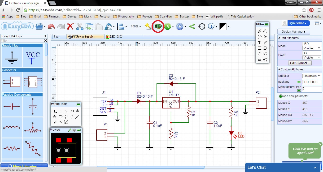
What is a PCB?

Un PCB (Printed Circuit Board), or printed circuit board, is a flat plate used in electronics to provide a mechanical and electrical basis for the connection and assembly of electronic components. They are essential as a base for connecting and holding components such as resistors, transistors, capacitors, diodes, microchips and other electronic devices.
A PCB is made up of:
- Substratum: It is generally a thin, flat layer of insulating material, such as fiberglass or epoxy resin, etc. This material provides structural support for the components and electrically insulates the conductive tracks.
- Conductive tracks– These are metallic patterns, usually copper, that are printed or etched on the surface of the PCB substrate. These tracks allow the conduction of electrical current between connected components.
- Metallic holes- Metallized holes are holes drilled into the substrate that are coated with copper, allowing electrical connection between different layers of the PCB or between components on different parts of the board.
- Surface Mount Components- We mean electronic components, such as resistors, capacitors, transistors, chips and other devices, are mounted on the surface of the PCB and connected to the conductive tracks to form electrical circuits by soldering.
- Welding mask and screen printing: It is a coating that is applied on the PCB to prevent solder from flowing out of the desired areas during the soldering process. Screen printing is used to label components and tracks on the PCB with visual identifiers.
PCBs can be single face (with conductive tracks on one side), double sided (with conductive tracks on both sides) or Multilayer (with multiple layers of conductive tracks separated by dielectric substrates), the latter being the most complex, as is the case of computer motherboards...
How a PCB is manufactured
La manufacturing of complex PCBs that we see on equipment such as computers, Smart TVs, mobile devices, etc., is quite complex. It consists of a series of steps that I will list here, but it must also be said that manufacturing a simple PCB is quite easy, and can be done at home with the products that we present to you in this article.
The followed used to manufacture a PCB are:
- Integrated
- PCB design using specific design software, such as EDA environments.
- Export of the design in Gerber format.
- Design verification, simulation to check its operation.
- Sending the file with the PCB layout to the factory.
- From layout file to film or mask
- Creating PCB films or masks from the design files.
- Using a plotter to print high-precision films.
- The films are developed and stored for later use in engraving processes.
- Printing of inner layers
- Printing the PCB design on copper sheets using photoresin to transfer the design.
- Exposure to ultraviolet light to harden the photoresist material into the pattern of the masks or films.
- Cleaning and verification of the PCB.
- Removing unwanted copper (etching)
- Chemical removal of unwanted copper through an acid bath process. The photoresin will protect the parts that you do not want to remove from the copper.
- Washing the PCB to remove acid and stop etching.
- Layer alignment and optical inspection
- Alignment of all layers using registration holes.
- Automatic optical inspection to detect defects.
- Union of layers
- Alignment and joining of the layers using prepregs (prepreg).
- Pressure and heat process to join the layers.
- Drilling
- Drilling precise holes in the plate by high precision CNC drilling machine.
- Identification of drilling points using X-rays.
- Copper plating and deposit
- Chemical deposition of a thin layer of copper on the plate.
- Copper is deposited in the drilled holes to interconnect the layers with each other.
- Image of the outer layers
- Application of photoresist on the outer layers using the corresponding mask.
- Exposure to ultraviolet light and removal of unhardened material.
- Plating
- Copper electroplating on exposed areas of the outer layers.
- Final etching or final engraving
- Removal of unwanted copper using a chemical solution.
- The tin protects the desired copper during this process.
- Solder Mask Application
- Application of an epoxy solder mask on both sides of the board.
- Curing the mask in an oven.
- Surface finish
- Electroplated with gold or silver to improve solderability, and some PCBs even receive pads for soldering.
- Serigraphy
- Printing important information on the surface of the PCB using laser or other printing.
- Test or test
- Automatic testing of PCB functionality and design compliance.
These steps are essential in PCB manufacturing and ensure the creation of high-quality printed circuit boards for use in a variety of electronic applications.
The best products for working with PCBs
Now that you know what a PCB is, let's look at some products you can buy to start designing and manufacturing them at home:
Laminated PCB

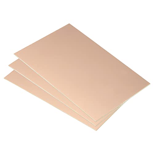

In the market you can find Laminated PCBs with a copper layer on one side or both, so you can engrave the circuit you need on it.
PCB support

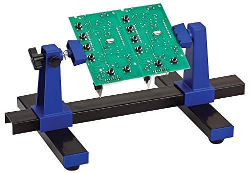

Another interesting product is this PCB support which will help you hold the board while doing tasks like soldering etc.
PCB Drill Bits


To drill holes on the PCB for mounting some components, you can use these special bits for your drill or for a CNC machine.
Protective varnish for printed circuits

Another recommended product is this varnish which you can apply in the form of a spray once you have finished the PCB. This will protect the surface.
Perforated plates


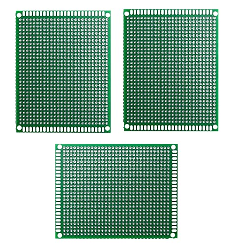
Also very useful are the perforated plates. With them, if you don't want to etch the laminated board, you can start soldering your circuit projects or practicing soldering.
Solder ink (mask)


It is used to apply as a solder mask, to protect the surface of the PCB, as I have described in the manufacturing process. You can easily apply it and then expose it to UV light to harden.
UV curing lamp


You can also buy a UV light curing lamp. These lamps are used to harden the ink or solder mask, for example, or to develop.
Flux or flux
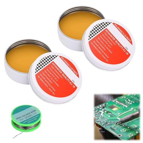


We already talked about what is flux or flux on another occasion, so I think it needs no introduction...
photosensitive film


For engraving you will need this type of photosensitive films to, using a mask, expose the areas you want to eliminate...
Acids for etching


To remove exposed copper from the laminated PCB, you will need a few sodium persulfate or ferric chloride acid baths like these. Of course, remember to take the necessary precautions when working with these chemical elements.

And don't forget to also use distilled and deionized water for rinsing, to eliminate the acid from the PCB by submerging the plate in a bath of this water after etching...
Thermal tape


Another product that can help you is these rolls of thermal tape, which can be used to protect some parts of the circuit. It can be used both to insulate some components or protect them from heat sources and to use them during welding to protect other parts from the heat generated in the process...
Plate for engraving

You probably also need these plates for Immerse the PCB in the acid during etching, and another one of these to use distilled water to wash the PCB once the etching has been carried out.
Acid resistant tweezers

And, finally, we also recommend some tweezers to be able to remove the PCB from the acid without using your fingers, since it would involve risk...